Overview
PCBs (Printed Circuit Boards) now form an integral part of any electronics system that you can find in your surroundings. This revolutionary technology has made it possible for us to make extremely complex circuits in very small area capable of performing a large number of functions for a long period of time without any compromise on reliability. Sysro Labs bring you the opportunity to learn the skill of designing a circuit using the required tools. Sysro Labs is looking forward to organize similar workshops in future to help Engineering students get familiar with relevant utility Technologies.
Idea of this workshop came into existence by understanding the industrial requirement and comparing it to the amount of practical knowledge to the students related to designing of circuit. This will also built a huge confidence in the students who are really interested in making and building their future in designing.
Course Details
>Each day is divided into 2 Sessions and thus a total of four sessions.
Session 1:
This session will include introduction to principle and working of different basic circuit that forms the building blocks of different type of electronic circuits. Techniques to combine and implement such basic circuit to form the schematic of any major project. Exposure to different types of electronic components & Sensor and there usage.
Session 2:
Introduction to different types of software for schematic designing, circuit simulation & PCB Layout Designing with their advantages & disadvantages. Hands-on practical on one of these software. Designing schematic diagram for one project, simulation and analysis of some projects using circuit simulation software, debugging & eliminating errors, Component selection criteria & PCB Layout Designing for the project, understanding techniques and tricks for circuit miniaturization.
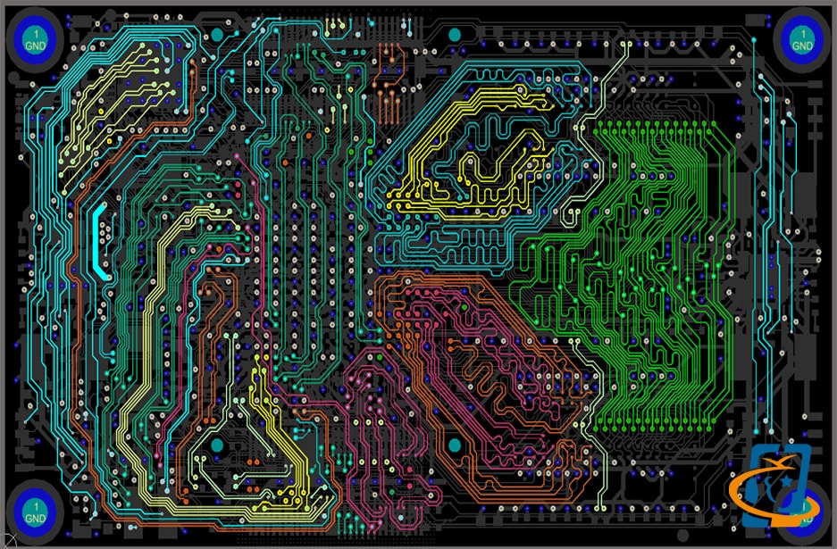
Session 3:
Techniques for developing double sided PCB, Parameter consideration for trace width, clad thickness, etc. Introduction to Surface Mount Devices and Device selection criteria for Surface Mount Technology (SMT) Type PCB. Developing Ground & Power Plane for single & Double sided PCB & designing tips for the same. Imprinting PCB tracks on copper clad, Explanation & Hands-on practical on Fabrication & Etching Process, Necessary tips regarding Component Assembly & Mounting Techniques, Soldering Techniques & Soldering Tips, Drilling the PCB & Soldering the components.
Session 4:
PCB testing and debugging and obtaining the expected result. Doubt discussion.
Register Now
Our Technologies